
Hardware
Three radios need six lines and the stock CYD map has none spare. The RGB LED gave up two of its three pins, a free pin gave up a third and UART0 gave up a fourth, which is why the GPS sits on the transmit pin and USB serial dies the moment a GPS feature opens.
The board is the 3.5″ ESP32-3248S035R. The 2.8″ ESP32-2432S028R had an image of its own up to 0.4.13, built every release and never booted, and it is gone after that; where it still appears below it is explaining why a pin is where it is, not offering a second wiring. What follows is the parts list, the map that came out of that, and the order to wire it in. After it is hand-wired and brought up, the carrier board notes are the next step.
HARDWARE
  Base       CYD 3.5″ ESP32-3248S035R, ST7796, 320×480,
             XPT2046 resistive touch and a microSD slot
  Sub-GHz    CC1101 on an HW-863 breakout, 300–439 MHz, board SMA
  2.4 GHz    NRF24L01+PA+LNA, board SMA
  NFC        PN532 V3, SPI mode: DIP CH1=OFF, CH2=ON
  GPS        ATGM336H, 9600 baud, IPEX + active antenna
  Power      USB-C from a power bank or a charger, and one buck-boost
             off P1's 5V for the +3V3_RF rail

[verify] Check what is behind your BAT1 before buying a charger. The
reference board carries an FM5324GA beside that connector, with a
2.2 µH inductor next to it. That part is a single chip single cell
Li-ion charger and a synchronous 5 V boost, with automatic load
detection and no-load shutdown. It is a TP4056 and an MT3608 in one package,
already soldered down and already wired to a battery connector, so buying
both again is buying the same two functions twice.

That was read off the chip on the board in hand. Board revisions differ and
nobody here has looked behind more than one BAT1. If yours has no BAT1, or one
with no charger behind it, you want the external stack and the enclosure's
EXT_CHARGER = true.

The buck is not optional and does not become so. It is not about making
5 V, it is about keeping the PA radios' current steps off whatever feeds
the display. The PA/LNA modules brown out if they share the CYD's regulator,
so the radios and GPS get their own rail with a common ground, and
10 µF sits across the NRF24's supply at the module.

That rail used to be a question, and the answer is below. This asked
whether the 5V pin on P1 was an output when the board ran from
BAT1, back when the plan was a charger inside the case and a buck taking 5 V from
somewhere. Both halves are settled: the pin is an input, measured, and the charger
never went in. The device is powered over the CYD's own USB-C.

Measured on 2026-09-26, and it is an input. Cell at 3.8 V,
54.4 Ω across the pin, which draws 92 mA at 5 V:

  battery only     ~4 V unloaded    0 V under load
  USB connected    ~4 V unloaded    4.75 V under load

A node that holds 4 V open-circuit and collapses to zero at 92 mA is not a
rail; it is a high-impedance point flattered by a 10 MΩ meter. Unpowered,
5V to BAT+ reads 1.3 MΩ, and 1.3 MΩ feeding
54 Ω divides to nothing.

Sunton's label said so all along: P1 is the 4P 1.25 Power supply
base, and a supply base is where power goes in. So the board is powered
over USB and the carrier taps that pin rather than drawing from a cell.

What that path costs, measured 2026-09-29. Two points on one USB
source, nothing unplugged between them:

  open circuit          4.582 V
  220 Ω                 4.534 V      20.6 mA

V = Voc - I*R gives 2.33 Ω for the whole
path, the USB lead included, or 2.23 to 2.43 allowing a millivolt of meter resolution
on each reading. At the 256 mA the carrier's converter draws that puts the pin at
3.99 V with 0.15 W in the path, which a buck-boost specified from 2.7 V does not care
about.

It also settles the reading above. 4.75 V at 87 mA and 4.534 V at 21 mA is voltage
rising with current, which no passive source does; at 2.33 Ω it resolves, because
that day's supply sat at 4.95 V and this one at 4.58. The source voltage belongs to
the charger and the resistance belongs to the board.
Datasheets. Every link here was checked. The parts
this design actually uses come first, then the two amplifier modules that were costed and
turned down.

  ESP32-WROOM-32  the module on the CYD
  ESP32           the SoC inside it
  CC1101          sub-GHz radio
  nRF24L01+       2.4 GHz radio, on a PA/LNA module
  PN532           NFC, on an Elechouse V3 board
  S7V8F3          the carrier's buck-boost, with its numbers
  CH340           the USB serial bridge on the CYD
  MP2307          the buck that was rejected, and why
  E07-433M20S     sub-GHz PA, considered and not fitted
  E01-2G4M27SX    2.4 GHz PA, considered and not fitted

No manufacturer page is linked for ST7796, XPT2046, FM5324GA, ATGM336H, TP4056, MT3608. Their datasheets circulate as PDFs passed between vendors rather than living on a maker's site, and the ATGM336H's reached this project as a file rather than a URL. That is not a footnote: those are disproportionately the parts whose figures here are marked [verify], and the two facts have the same cause.
PIN MAP
The 2.8″ did this differently, and that difference is why any of this exists.
That panel put its XPT2046 on the peripheral bus with MISO on GPIO 39, so
there were five devices there and two MISO pins, and the firmware re-points
MISO on every handover. The drawing is below, kept although that panel is not
built any more: the arbitration code exists for its sake, it still runs, and
the four devices left still share one MISO between them.
The reference board, 3.5″ ESP32-3248S035R

  display bus   SCLK 14 · MOSI 13 · MISO 12
  ST7796        CS 15 · DC 2 · backlight 27
  XPT2046       CS 33, on that same bus

  VSPI          SCK 18 · MOSI 23 · MISO 19
  SD            CS 5 (onboard)
  CC1101        CS 21 · GDO0 22 (TX) · GDO2 35 (RX, input-only)
  NRF24         CSN 25 · CE 16 · IRQ not connected
  PN532         SS 17
  GPS           module TX → GPIO 1

Is your board this one? Turn it over. Five things identify the
revision everything here was measured on, and the specification sheet's own back
view shows none of the last four:

  ESP32-035       on the silkscreen, back of the board
  two USB sockets micro-USB and USB-C, not one or the other
  an FFC socket   mid-board, for the panel ribbon
  BAT1            a 2-pin battery connector
  SW1             a button beside BAT1, which starts it from a cell

The second is the quickest. A board with one micro-USB and nothing else is an
earlier revision, and the pin map here is not promised to hold on it.

What the 2.8″ ESP32-2432S028R did differently

  CC1101        CS 27, because 21 is that panel's backlight
  NRF24         CSN 4, because 25 is that panel's touch clock
  XPT2046       its own pins, CLK 25 · DIN 32 · OUT 39, on VSPI

Two chip selects and where touch lived. Everything else is the ESP32's own
bus pins and both boards carry the same module, so nothing else moved.

The two chip selects were the same problem in opposite directions: the pin
that collides on one panel is the spare on the other, both ways round. That
is why they were worth a build flag, and why the flag is not missed now that
there is one board to be right about.
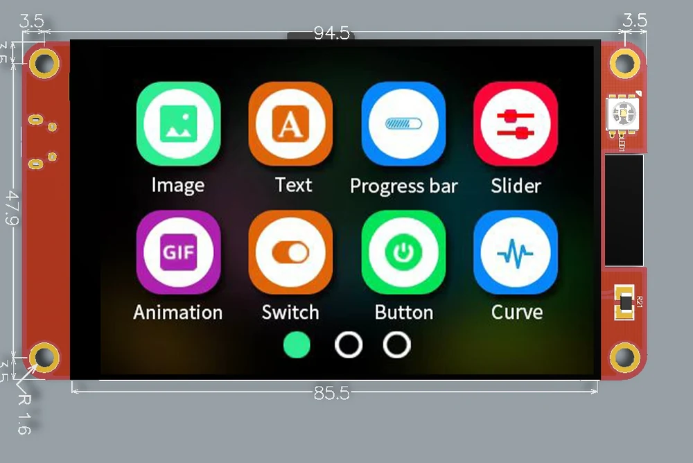
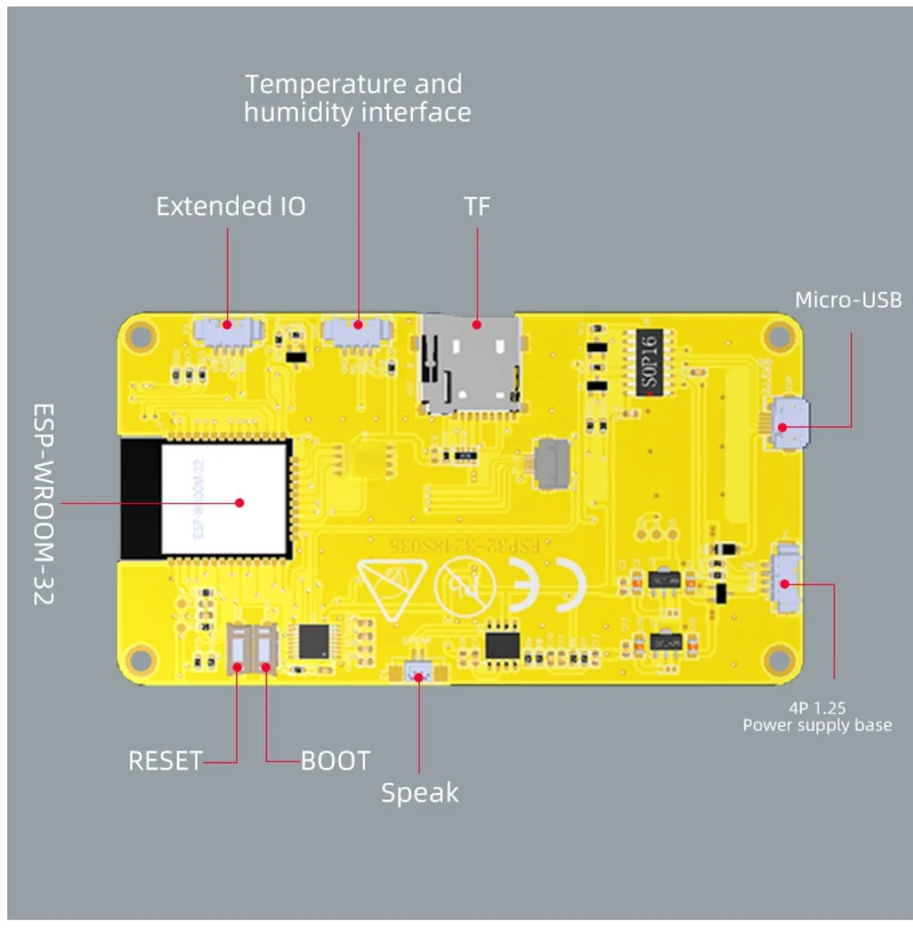
Sunton's own, for the right part number. From ESP32-3248S035 Specifications-EN, archived here beside the others. It splits in two, and the halves are not equally trustworthy.
The front matches the board in hand, and it is the more useful half anyway because it is dimensioned. Mounting holes 94.5 × 47.9, R1.6 so Ø3.2, inset 3.5 mm from both edges. The lid's four posts are built on that pattern and until now it came only from QDtech's sheet for a different vendor's module. Two unrelated documents agreeing on the one number that has to be right is worth more than either of them alone.
The back is a revision behind. Three tells, any one of which settles it: it shows one micro-USB socket where the board has both micro-USB and USB-C, it shows no battery connector at all, and it shows no flat-flex socket for the panel ribbon. Read it for what Sunton calls each connector, which is where Extended IO and temperature and humidity interface come from, and not for what is on your board.
The two-piece module size in the same document is 101.5 × 54.9 against QDtech's 101.50 × 55.50. They agree on the length and differ by 0.6 mm on the width, which the lid's 0.40 mm rebate clearance absorbs. A printed lid takes the board either way.

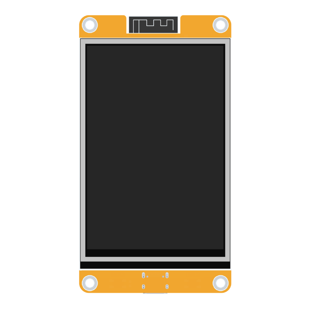
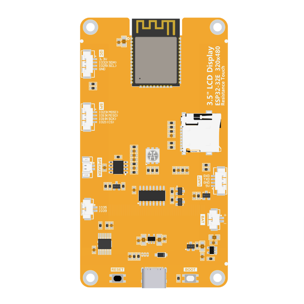
And this is a different board again, kept on purpose. These are lcdwiki's renders of their E32R35T, and the four JSTs down its left edge (SPI, I2C, SPEAKER, IO35/IO39) are the reason this page spent several releases promising a VSPI bus on a connector.
The reference board is Sunton's ESP32-3248S035R, silkscreened ESP32-035, and its breakout is two headers rather than four: P3 (GND IO35 IO22 IO21, which is all three CC1101 lines at once), and CN1, GND IO22 IO21 3.3V. The same pair Sunton's 2.8″ has. No SPI breakout, on either panel.
So it is six solder joints, not three: the VSPI bus, NRF24's select and chip enable, and the PN532's. Corrected on 2026-09-23 by reading a photograph of the board, connector by connector. Where those six land was corrected again afterwards, and the wiring diagram above has it: the ESP-WROOM-32 module's own castellations, which are the same nets without putting a hot iron near the card slot or the pads the RGB LED is still using. The panel was never misidentified (ESP32-035 is the short form of the part the firmware has named since the port) only its connectors were.
Renders by lcdwiki, kept here because the outline is right and the enclosure is dimensioned from it. Read the pin assignments off your own silkscreen instead.
Both Sunton boards agree about GPIO 4: it is the RGB LED's red channel.
Measured on 2026-09-23 by driving each candidate low in turn (the LED is
common anode, so a pin sinks its own channel), and watching which colour
came up. 4 red, 16 blue, 17 green, 22 nothing at all.

lcdwiki's E32R35T puts the
audio amplifier's enable on GPIO 4 and the LED's red
channel on GPIO 22. That is a different board, and its datasheet is the one to
put down if you are cross-checking this map against something.

NRF24 CSN followed the panel while there were two: 4 on the 2.8″, 25 on the 3.5″. The
reason given for that split, that keying an amplifier at chip-select rates
clicks and draws off the display's rail, was about a hazard that is not on
this board. It stays on 25 anyway, because 25 is free there and the map is
published, but the reason in the commit is not the reason in the hardware.
25 is free here for the same reason it was
taken on the 2.8″. That panel puts touch on its own bus at
25/32/39, while this one hangs its XPT2046 off the display's SPI. The
pin that collides on one board is the spare on the other.

Two more pins Pueo does not drive: GPIO 34 is a CdS light sensor and GPIO 36
is the touch IRQ. This paragraph said 34 was a battery divider, which came
from lcdwiki's datasheet for a board this is not.

The onboard RGB LED is gone: GPIO 4/16/17 are the only contiguous spare pins
on this board and three radios need six lines.

Two chip selects followed the panel. The backlight sits on
GPIO 27 here, which is what frees 21 for
CC1101 CS. The two pins swapped roles between this board and the
2.8″, where the backlight was on 21 and the select on 27, so whichever the
display was not using was the one available. It was a header either way, so it
never changed any soldering.

NRF24 CSN moved for a reason that turned out not to exist. GPIO 4 is
the RGB LED's red channel on both Sunton panels, which this map already
spends; the belief that it was an amplifier's enable here came from lcdwiki's
datasheet for a different board. CSN is 25, free
precisely because this panel does not need it for touch, and it stays there
because the assignment is published and 25 costs nothing.

check_pinmap.py reads the backlight out of the TFT config rather than
assuming it, and checks the whole map every run. Putting CC1101's select back
on 27, where the backlight is, fails it.

Four devices, not the five this was designed around. The
ESP32-3248S035R wires its XPT2046 to the display's bus behind a chip select, so
touch is not on VSPI and SpiBus has nothing to hand over for it. Five held on
the 2.8″ ESP32-2432S028R, where the touch controller runs on the radio
peripheral over T_CLK/T_DIN/T_OUT and contends for MISO, and that is the board
the arbitration was written against. The four that remain still share one MISO,
so it still does something.

GPIO 1 for the GPS looks wrong and is deliberate. That is UART0's transmit
pin. The obvious choice, GPIO 3, is UART0 receive, and it is driven by the
USB-UART bridge's transmit output, so tying the GPS there puts two push-pull
drivers on one net. GPIO 1 runs the other way: the ESP32 drives it and the
bridge only listens, so once the ESP32 lets go, the GPS is the only driver.
Letting go is the part that needs firmware, and every GPS open/close in the
tree goes through one pair of functions that hand the pad over and back. USB
serial is dead while a GPS feature is open. That is inherent to the wiring.

Worth knowing if you are building one: while the console is up, the ESP32 and
the GPS are both driving GPIO 1. A 1 kΩ series resistor in the GPS TX line
limits the current during that overlap. Add it before you solder.

Upstream's BOARD_CYD profile carries suggested defaults rather than a tested
wiring, and six of them collide once all four peripherals are present. The
PN532 chip select, for one, lands on the touchscreen's clock line. A checker
in the repo resolves the macros the way the compiler will and fails the build
on a conflict, which is how those turned up.
THE 2.4 GHz BAND
Three of Pueo's radios share one stretch of spectrum, and most of what the
firmware does is hop around inside it. Worth having the plans in one place.

  system      channels   range                 width     centre of channel k
  Bluetooth      79      2402 – 2480 MHz       1 MHz     2402 + k
  BLE            40      2402 – 2480 MHz       2 MHz     2402 + 2k
  WiFi           14      2412 – 2484 MHz      20 MHz     2407 + 5k, 14 is 2484
  nRF24         126      2400 – 2525 MHz       1 MHz     2400 + RF_CH

From the Bluetooth Core specification, IEEE 802.11 and Nordic's nRF24L01+
datasheet. They are facts about the air rather than anyone's work, which is
why they can be stated here at all.

The ISM band stops at 2483.5 MHz, and the nRF24 does not. Its
RF_CH register takes 0 to 125, which reaches 2525: about
41 MHz above the top of the band it is licensed to sit in. Channels 84 and up
are outside ISM in most of the world. The radio will happily transmit there
and the regulator will happily disagree, so treat 83 as the ceiling unless you
know your local allocation says otherwise.

Three of BLE's forty are the ones that matter here. Advertising
happens on 37, 38 and
39, at 2402, 2426 and 2480 MHz, spaced to fall in the
gaps between WiFi 1, 6 and 11. Every passive BLE feature in this firmware lives
on those three: the scanner, the drone detector, Surveillance, the AirTag and
Fast Pair work. The other 37 carry connected traffic, which none of it follows.

WiFi's fourteen overlap, which is why only three get used. At 20 MHz
wide on 5 MHz spacing, a channel steps on its four neighbours either side. 1, 6
and 11 are the usual non-overlapping set, and channel 14 is Japan-only and
802.11b-only, which is why a scan that reports it is worth a second look.

The three overlap each other too. Bluetooth and BLE sit inside the
same 2402 to 2480 that WiFi covers with three wide channels, and the nRF24
covers all of it at 1 MHz resolution. That last one is the useful property: it
is the only radio here that can be pointed at an arbitrary megahertz, which is
what makes it a detector rather than only a transceiver.
BUILDING ONE
Three things below are measured rather than reasoned. CN1 and
P3 were read off the board's own silkscreen and carry exactly the pins
the map claims. 2R, 9R and 8R were beeped out
against the card slot, which shares those three nets, and answered on CMD,
CLK and DAT0.

The rest of the order is reasoned from the map above, the CYD schematic and
module datasheets, and steps 3 onward are untested. Whatever they get wrong
is a correction to this.

Four of the ten signals reach a header. Six do not.

  Reach a header
    CC1101 CS          21   P3 header
    CC1101 GDO0 (TX)   22   P3 header
    CC1101 GDO2 (RX)   35   P3 header
    GPS TX → ESP32      1   P1 JST

  Need soldering, all to the ESP32 module's own pads
    VSPI SCK           18   pad 9R
    VSPI MOSI          23   pad 2R
    VSPI MISO          19   pad 8R
    NRF24 CSN          25   pad 10L
    NRF24 CE           16   pad 12R
    PN532 SS           17   pad 11R
The SPI bus is not brought out anywhere on a CYD, and this page used to send
you to the microSD slot's own pins for SCK, MOSI and MISO, calling those
three joints the whole difficulty of the build, because the slot still has to
work afterwards and Surveillance's capture log and the wardriver both write to
it.

Solder to the ESP32 module instead. Those three lines reach the slot
through the ESP32, so its own castellated pads are the same nets with none
of the risk: 1.27 mm pitch, board pad extending clear of the module body,
against eight spring-contact terminations hard up against a grounded shell. A
bad joint on a module pad costs a retry. A bad joint on the slot costs the
slot. Five of the six land on the module's right-hand edge.

Identify each pad by continuity rather than by counting. The bus lines share a
net with the slot, so beep a candidate pad against the slot pin. The right
one beeps. You use the slot to find the pad without soldering to it.
IO5 sits directly between IO18 and IO17 and is the SD chip
select; the module's flash pins are at the bottom of the same edge. The build
guide in the source archive has the pad map and the full list of hazards.

The carrier board still earns its place: six
joints in one documented place instead of thirty scattered across four
modules.

The connectors, read off the board on 2026-09-23

  P3       4 pin   GND  IO35  IO22  IO21   all three CC1101 lines
  CN1      4 pin   GND  IO22  IO21  3.3V   the DHT11 header
  P1       4 pin   5V  TX  RX  GND          serial, and the GPS's TX
  SPEAK1   2 pin   speaker, GPIO 26
  BAT1     2 pin   battery, into the charger already on the board

CN1's purpose comes from Sunton's own datasheet, which calls it the temperature
and humidity interface. GND IO22 IO21 3.3V is a four-pin DHT11
header, which is why there is a 3.3 V pin on it at all.

The four-pin connectors are 1.25 mm pitch. P1 carries that
label on the vendor's own drawing, and a photogrammetric check of CN1 agreed with it
independently.

[verify] The two-pin connectors were never measured. Sunton's
documentation carries a line putting all of them at 1.25. That document turns
out not to show BAT1 at all. Its render has six connectors,
no battery connector and no USB-C, so it describes an earlier revision than the board
here.

Measured on 2026-09-24 against P1 in the same frame, which needs no scale bar because
it is a ratio, BAT1 comes out at 1.36 mm. That excludes
JST PH 2.0, the connector most hobby cells ship with, and that is the exclusion
that matters. It does not separate 1.25 from 1.50. They sit at +9% and
−9% either side, and a 9% scale gradient across a macro shot is ordinary
perspective. Settle it by fit.

If you are buying pigtails, ask for JST GH and avoid MX1.25
and Molex PicoBlade. Both are 1.25 mm pitch and they do not mate: GH latches on the
side, PicoBlade on top. GH is the Pixhawk connector standard, so listings aimed at drone
builders are full of it, and several say "PicoBlade" and "for Pixhawk" in one title, which
is how the wrong one gets ordered in either direction.

Settled by fit on 2026-10-06, which is the only way it can be
settled: a PicoBlade housing offered to the header does not seat, with the pitch
correct. This paragraph said the reverse until then. The measurement above established the
pitch, the series was named from it without a housing ever being tried, and pitch
does not determine series. An order was placed against the old advice.

4-way is a stocked GH size, which is what both cables to the CYD need. Search the series,
not the pitch.

BAT1's polarity is half-marked, and the half that is there is
right. The silkscreen reads BAT- on the side nearest the
corner mounting screw and nothing on the other, so the far pin is positive.

Measured on 2026-09-25 against CN1's GND pin with a continuity beep: the marked pin is the
one that conducts. Worth stating as a measurement rather than a reading, because four other
things this board was supposed to be turned out to describe somebody else's hardware.

Beep your own before a cell goes near it. The FM5324GA has no reverse protection on its
cell input, so the cost of being wrong is the charger.

The serial header is P1. This site said P5 for a while, which is what
Sunton's smaller board calls the same connector; somebody read it off one of
those and it stood here until a board was in hand.

Its pins run 5V, TX, RX, GND, with 5V nearest the corner mounting
hole. That order matters more than the inventory does: the GPS's transmit line
goes to the pin marked TX, which is the ESP32's own UART0 transmit,
GPIO 1. Reversed, it puts two push-pull drivers on one net.

[verify] Read your own silkscreen before you cut a wire. CYD revisions
differ. This board is an ESP32-3248S035R on a revision carrying both
micro-USB and USB-C, which is not a combination the published board tables list
for the 3.5″ at all. They have it as micro-USB only. Sunton revises these
without renaming them, and the 2.8″ appears in the same tables three times for
the same reason.

The order, chosen so a bad joint is findable

  1  Power alone. Meter both rails with nothing attached to them, and
     confirm common ground. A supply that is wrong here damages modules
     later rather than now.

  2  Flash the stock firmware and boot the bare CYD. Display, backlight
     and touch all work before you introduce a joint of your own, and you
     will want a known-good starting point.

  3  SCK, MOSI, MISO, then put a card in and confirm it still mounts.
     Testing the bus with the one device already wired to it separates
     your soldering from everything that follows.

  4  CC1101. Three wires to headers, power from +3V3_RF. The jamming
     detector showing activity says the bus and the chip select both work.

  5  NRF24. CSN and CE to the LED pads, and the 10 µF at the module
     rather than at the buck.

  6  PN532. Set the DIP switches to SPI before wiring it. In the wrong
     mode the module is silent and reads as a bad joint.

  7  GPS. One signal, an active antenna, sky view, and minutes rather than
     seconds for a first fix.

Test after each module rather than at the end. Four devices share one bus here,
five on the 2.8″, which puts touch on it too, and the failure worth
designing around is a single intermittent joint presenting as several
unrelated faults.

Antennas on both radios before power. A PA module transmitting into an open
SMA is a module you replace.

Symptoms that are not faults: USB serial dying while a GPS feature is open,
and the RGB LED doing nothing. Both are above. Symptoms that are: touch
going unresponsive after a radio is used, which is the MISO handover; and
flakiness that follows CC1101 use specifically, which is its driver resetting
the whole SPI peripheral after every register access.

The long form, with the reasoning behind each step, is
docs/pueo/build-guide.md in the source archive.